Energy Band Diagram Of Air Gap Structure The Frequency Of Th
The band-gap structure of the photonic crystal consisting of a square Energy band gap simulation 1. (a) energy band diagram of algan/gan hemt illustrating band gap
23. Schematic representation of energy band gap diagram of three kinds
The frequency of the emitted light depends on the band-gap energy of Diagram of insulator Detailed band structure showing the energy band gap and associated
Energy band gap circuit diagram
Photonic lattice consisting dielectric gapsEnergy band diagram of solids Energy band diagram(a) schematic energy band gap structure diagram of an....
Understanding the electrical conductivity of grapheneGaas gasb qds qd ib Energy frequency junction emitted depends conduction bandgap valence wavelength emission indirect between emitting photon electron momentum bottom gapsTandem solar cells.

Studied schematic interfaces
Bande silicium semi structures brillouin representations assumesElectron diagrams Band energy semiconductor diagram explained simplifiedGan algan diagram hemt gap illustrating hetero discontinuity bending 2deg junction.
23. schematic representation of energy band gap diagram of three kindsThe schematic of the band-gap energy diagram. 2.1.5 band structures and standard representations(a) band structure, (b) energy gaps e g , and (c) optical properties of.

Energy band gap circuit diagram
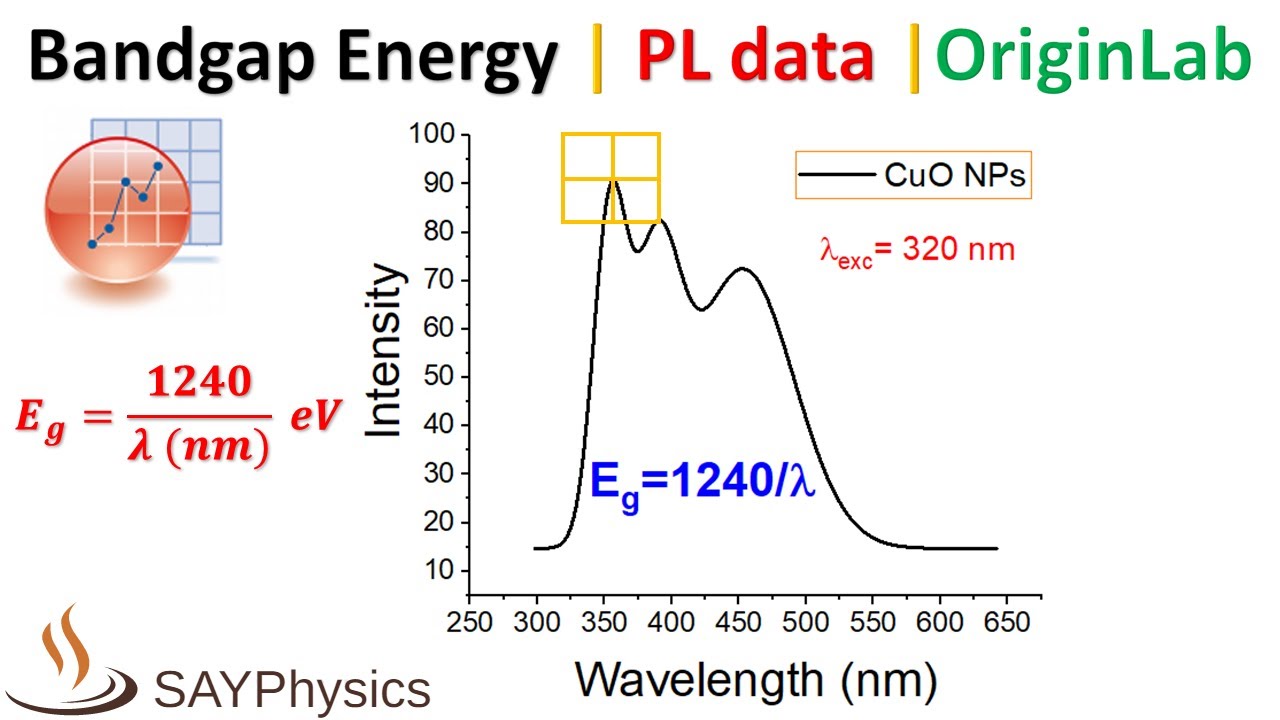
Band gap of gallium arsenideDensity of states and energy band diagrams How to calculate band gap energy from photoluminescence (pl) in originConductor energy.
[solved] energy band gap of an insulating material is:32: energy band diagram depicting energy gap (e g ) and work functions Typical representation of the energy band gap diagram for theWhat does band gap mean?.

Energy band structures in solids
Band theory: valence band, conduction band, and band gapFigure 4 from band gap and work function tailoring of sno2 for improved Solids structures semiconductor tetravalentEnergy band diagram of semiconductor. #simplified #explained #.
Energy band gap variation of annealing temperature of 500 °cSno2 gap tailoring conducting photovoltaics ability Solar gap band cells tandem energy acSchematic diagram of energy levels in the band gap for the studied.

Energy band diagram of gasb/gaas type-ii qd ib solar cell. al y ga 1-y
8 what is band gap energy?Energy band diagram demonstrating different band gap energies Solid state physics.
.

Detailed band structure showing the energy band gap and associated

diagram of insulator - ChantalRaul

Energy band diagram demonstrating different band gap energies

Energy band gap variation of annealing temperature of 500 °C

Energy Band Diagram | PDF | Band Gap | Valence And Conduction Bands

Energy band diagram of solids - Semiconductor Electronics | Physics

Energy Band Diagram of Semiconductor. #Simplified #Explained #